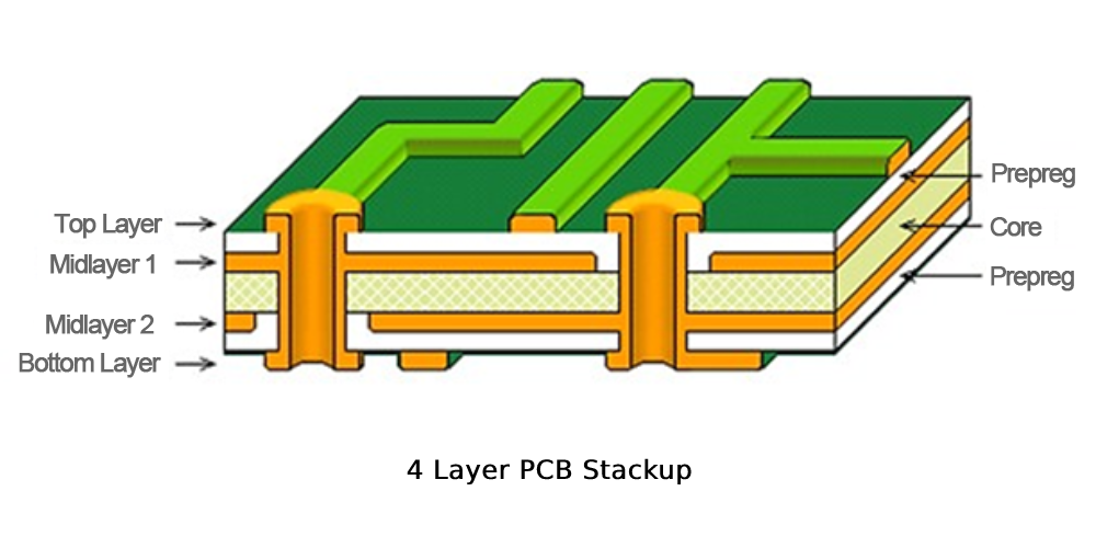
Understanding Proper Stackup Procedures With These Comprehensive 4 Layer Pcb Design Rules For Modern Electronics Manufacturing - Mastering 8 layer pcb stackup design
If you are searching about 4-Layer PCB Design Guidelines: Key Tips for Success | Viasion you've visit to the right place. We have 35 Pictures about 4-Layer PCB Design Guidelines: Key Tips for Success | Viasion like 4-Layer PCB Design Strategies - VSE, 4-Layer PCB Design Guidelines: Key Tips for Success | Viasion and also 4 Layer Flex PCB: Design and Manufacturing Guide- Jarnistech. Here it is:
4-Layer PCB Design Guidelines: Key Tips For Success | Viasion
 www.viasion.com
4-Layer PCB Design Guidelines: Key Tips for Success | Viasion
PCB Stackup Design Guidelines - MOKO Technology
 www.mokotechnology.com
PCB Stackup Design Guidelines - MOKO Technology
Multilayer PCB Stackup Planning - Artist 3D
 artist-3d.com
Multilayer PCB Stackup Planning - Artist 3D
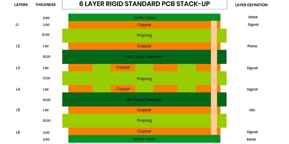
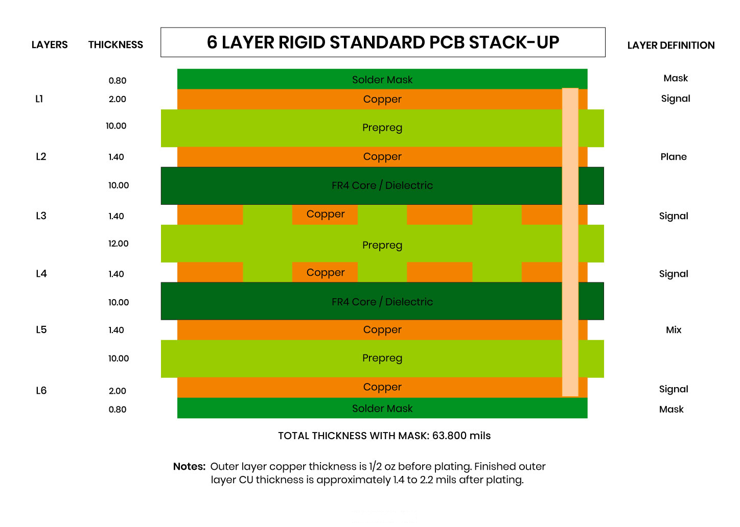
Understanding The Fundamentals Of 6-Layer PCB Stackup Design
 hilelectronic.com
Understanding the Fundamentals of 6-Layer PCB Stackup Design
Key Points In The Design Of 4 Layer PCB | Viasion
 www.viasion.com
Key Points in the Design of 4 Layer PCB | Viasion
PCB Stackup Design Guidelines - MOKO Technology
 www.mokotechnology.com
PCB Stackup Design Guidelines - MOKO Technology
PCB Stack-Up Guide & Examples | San Francisco Circuits
 www.sfcircuits.com
PCB Stack-Up Guide & Examples | San Francisco Circuits
PCB Stackup Design: A Comprehensive Guide From Basics To High-Speed
 www.ugpcb.com
PCB Stackup Design: A Comprehensive Guide from Basics to High-Speed ...
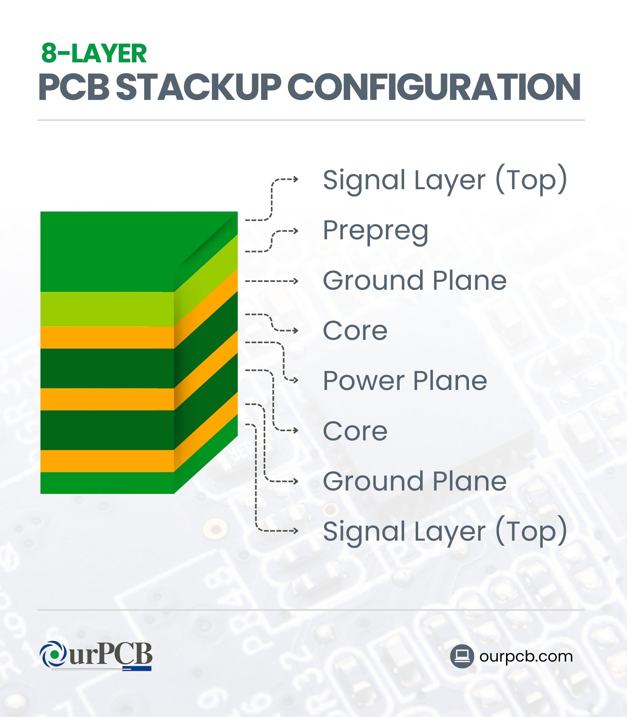
What Is An 8-Layer PCB Stackup? Examples And Guidelines
 www.ourpcb.com
What is an 8-Layer PCB Stackup? Examples and Guidelines
4-Layer PCB Design Strategies - VSE
 www.vse.com
4-Layer PCB Design Strategies - VSE
4-Layer PCB Design Guidelines: Key Tips For Success | Viasion
 www.viasion.com
4-Layer PCB Design Guidelines: Key Tips for Success | Viasion
PCB Stackup Planning - Simple - Artist 3D
 artist-3d.com
PCB Stackup Planning - Simple - Artist 3D
What Is RF Circuit Design? | Getting Started | Altium
 resources.altium.com
What is RF Circuit Design? | Getting Started | Altium
Understanding The Layer Stackup For Optimal ECU PCB Performance
 www.allpcb.com
Understanding the Layer Stackup for Optimal ECU PCB Performance
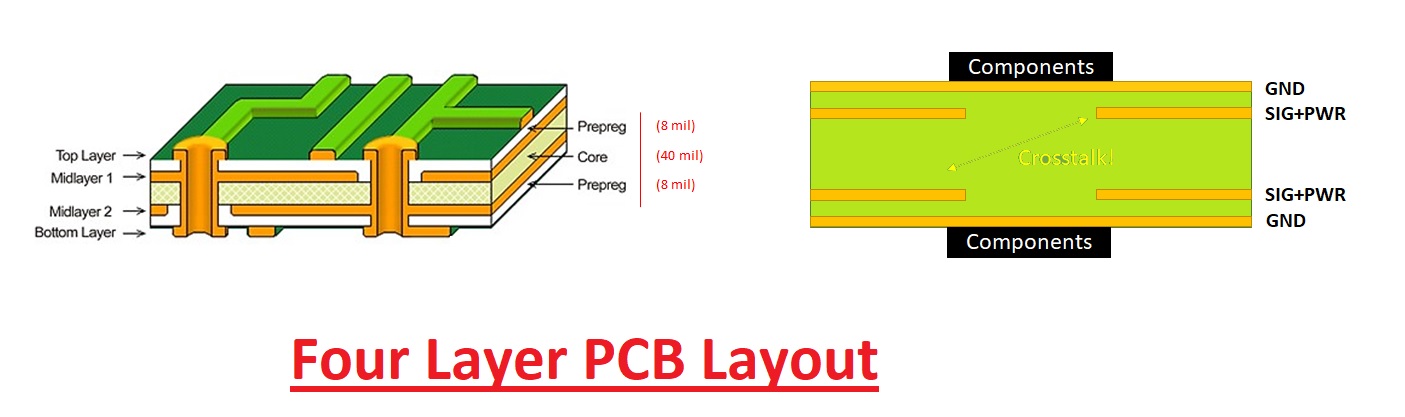
Four Layer PCB Layout: Design Process And Cost Of Manufacturing
 www.theengineeringknowledge.com
Four Layer PCB Layout: Design Process and Cost of Manufacturing
What Is An 8-Layer PCB Stackup? Examples And Guidelines
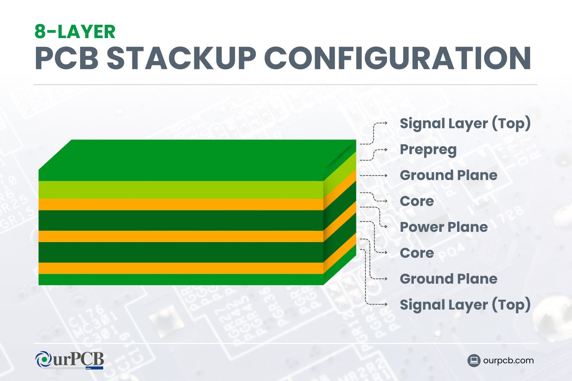 www.ourpcb.com
What is an 8-Layer PCB Stackup? Examples and Guidelines
PCB Stackup ExplainedHow To Plan A Multilayer Stack
 southelectronicpcb.com
PCB Stackup ExplainedHow to Plan a Multilayer Stack
4-Layer PCB Design Guidelines: Key Tips For Success | Viasion
 www.viasion.com
4-Layer PCB Design Guidelines: Key Tips for Success | Viasion
Mastering 8 Layer PCB Stackup Design - A Comprehensive Guide - JHYPCB
 www.pcbjhy.com
Mastering 8 Layer PCB Stackup Design - A Comprehensive Guide - JHYPCB
4 Layer Flex PCB: Design And Manufacturing Guide- Jarnistech
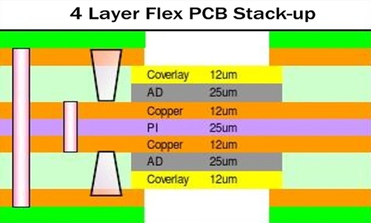 www.jarnistech.com
4 Layer Flex PCB: Design and Manufacturing Guide- Jarnistech
Layer Stackup: A Comprehensive Guide To Printed Circuit Board Design
 www.linkedin.com
Layer Stackup: A Comprehensive Guide to Printed Circuit Board Design
PCB Stackup Design Guidelines - MOKO Technology
 www.mokotechnology.com
PCB Stackup Design Guidelines - MOKO Technology
PCB Prepreg: A Comprehensive Guide - MorePCB
 morepcb.com
PCB Prepreg: A Comprehensive Guide - MorePCB
PCB Layers Introduction: Stackup, Thickness, Applications
 www.fcpcba.com
PCB Layers Introduction: Stackup, Thickness, Applications
Understanding 6-Layer PCB Stackup: A Comprehensive Guide - VictoryPCB
 www.victorypcb.com
Understanding 6-Layer PCB Stackup: A Comprehensive Guide - VictoryPCB
4 Layer PCB Stackup: Thickness, Cost & Manufacturing Process
 www.technotronix.us
4 Layer PCB Stackup: Thickness, Cost & Manufacturing Process
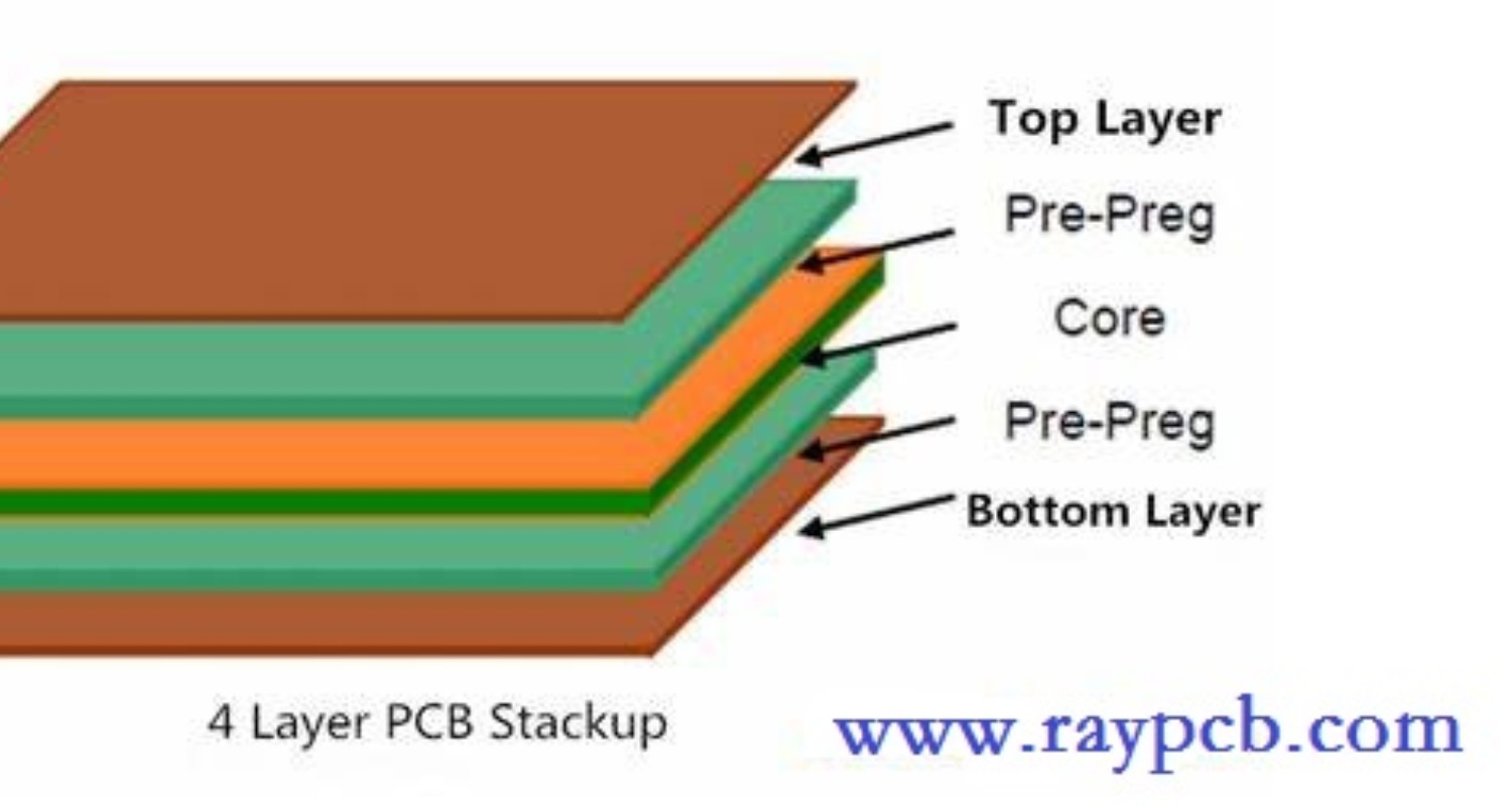
RAYPCB -standard-stackup-for-multilayer-pcbs – RF PCB
 rfpcb.org
RAYPCB -standard-stackup-for-multilayer-pcbs – RF PCB
Four Layer PCB Layout: Design Process And Cost Of Manufacturing
 hackaday.io
Four Layer PCB Layout: Design Process and Cost of Manufacturing ...
14 Layer PCB Stackup: A Comprehensive Guide | Viasion
 www.viasion.com
14 Layer PCB Stackup: A Comprehensive Guide | Viasion
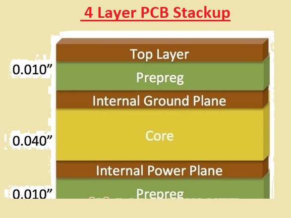
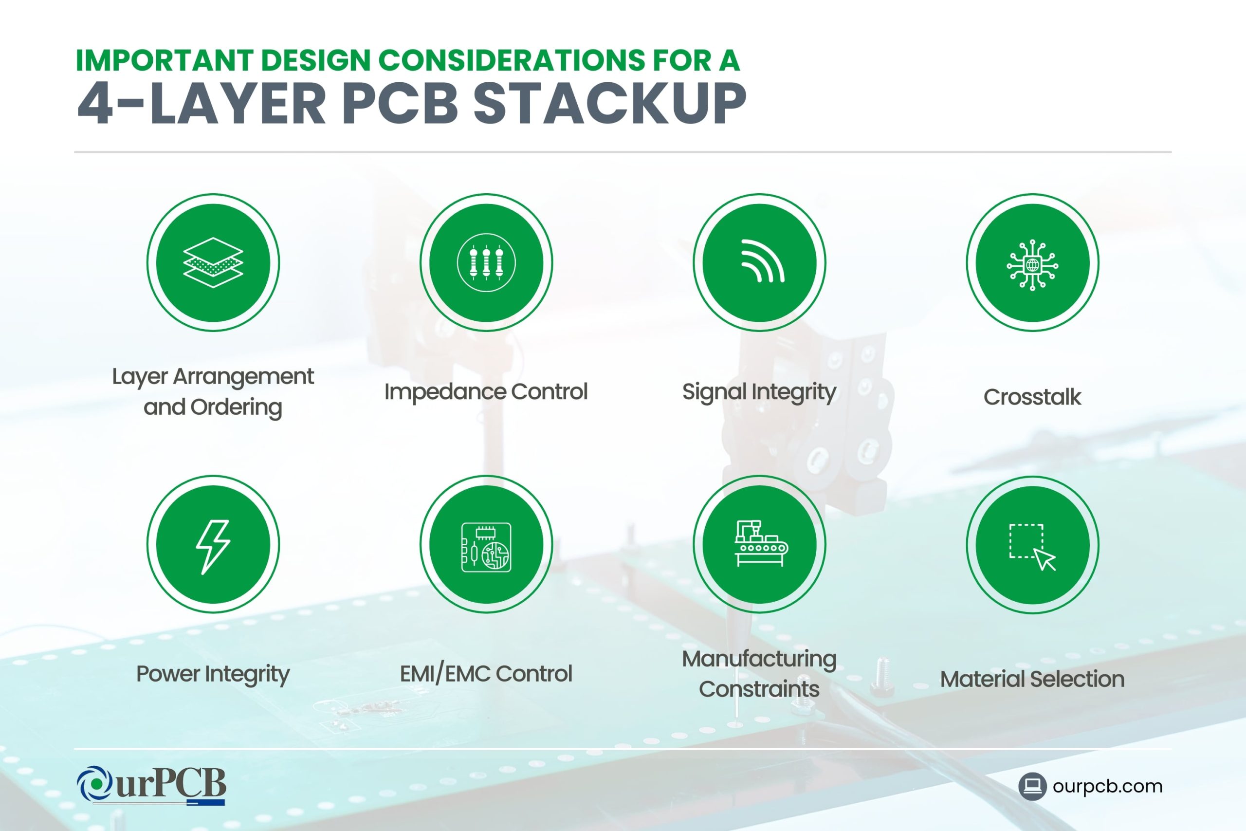
What Is A 4-Layer PCB Stackup? Examples & Guidelines
 www.ourpcb.com
What is a 4-Layer PCB Stackup? Examples & Guidelines
Understanding PCB Jumpers: A Comprehensive Guide
 www.fscircuits.com
Understanding PCB Jumpers: A Comprehensive Guide
PCB Stack-Up Guide & Examples | San Francisco Circuits
 www.sfcircuits.com
PCB Stack-Up Guide & Examples | San Francisco Circuits
Understanding PCB Capacitor : Types, Functions, And Applications In
 www.mainpcba.com
Understanding PCB Capacitor : Types, Functions, and Applications in ...
Basic Rules Of PCB Design For High-Quality Circuit Boards
 hilelectronic.com
Basic Rules of PCB Design for High-Quality Circuit Boards
Advanced GD&T And Tolerance Stack Up Analysis Workshop By Tetrahedron | PDF
 www.slideshare.net
Advanced GD&T and Tolerance Stack up Analysis Workshop by Tetrahedron | PDF
pcb stackup explainedhow to plan a multilayer stack. 4-layer pcb design guidelines: key tips for success. pcb stackup design guidelines